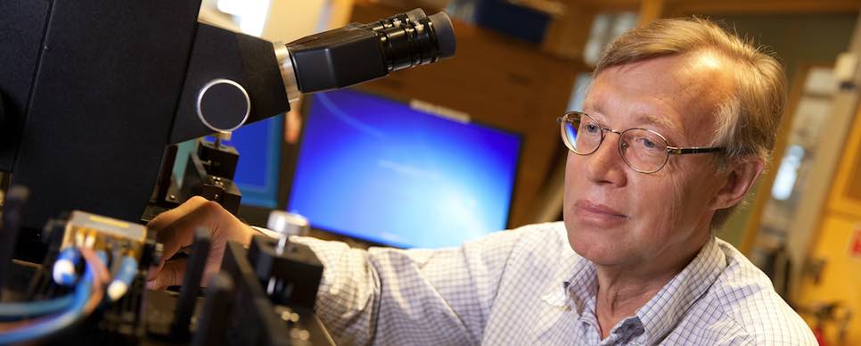
 30 years ago Herbert Zirath was one of the founders of the first electronics laboratory at Chalmers University of Technology. Today he is a professor of high speed electronics with responsibility for the Microwave Electronics Laboratory, which is housed in the university’s well-known MC2 laboratory. He also operates as a bi-directional knowledge conduit for Ericsson, where he is employed part-time as an expert on microwave circuits. The projects he presides over are almost limitless, but one clear objective is to create spectrum-efficient wireless communication in order to achieve ever higher data rates.
It is impossible to provide a brief summary of Zirath’s career. After a few hours in his company this becomes clear. Instead, you have to cherry-pick from his densely packed portfolio, which started to take form more than 35 years ago when, at random, he started working on microwaves as a doctoral student at Chalmers.
A common thread in his research has been the development of transistors with a higher and higher cut-off frequency. By combining materials with different band gaps, electrons can be made to move in a material without doping, thus increasing the speed.
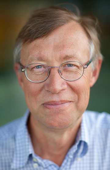 |
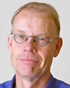
| Herbert Zirath |
“This is called band-gap engineering. It involves the development of artificial semi-conductor structures that have the characteristics we are seeking. We’ve been working on this since we made the first transistor in the lab here at Chalmers,” Zirath explains.
He received his first grant for transistor development in 1986. Prior to that he had simulated and started producing diodes for frequency mixers up to 140 GHz with an eye to the Onsala Space Observatory, and also dived into Schottky diodes.
“This was how we started to build up our knowledge of components. We made diodes from gallium arsenide, which were also developed here at Chalmers.”
At the same time as the interest in transistors took over Zirath started to set up a small laboratory with Anders Larsson, who is now a well-known Chalmers professor in photonics. Together they bought the university’s first ultra high vacuum evaporation system for deposition of the titanium-platinum-gold metal gate of the transistor.
“It was a pioneering era,” laughs Zirath.
World record circuit in millimetre-wave link
Over the years the focus of his research has moved from transistor level through circuits and on to systems. It applies to each material the group has studied and is studying – from gallium arsenide, through indium phosphide, to III-nitrides such as gallium, aluminium and indium nitrides.
Transistor development is important, but there is always a circuit in mind and for that some sort of application in communications or sensing.
“Ideally you want to have control of the entire chain, from materials to systems, but that’s easier said than done. Take a microwave link for example. It contains a great deal more than the front-end parts and includes the baseband, processor components and so on. This makes it so interesting to work with companies with systems expertise.”
Most of Zirath’s research is carried out in collaboration with industry. The Chalmers group develops a new circuit, while industry provides a system perspective.
This is also where the lion's share of the funding comes from – for example, projects are supported by the Swedish Foundation for Strategic Research (SSF), the Swedish Research Council, Vinnova or the EU, with co-funding from industry.
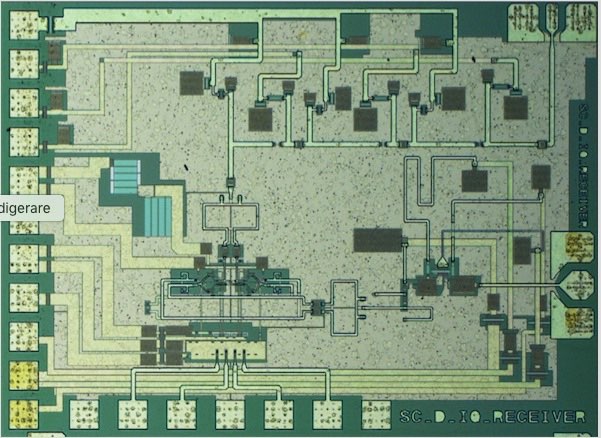 |
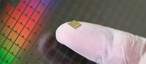
| The chip that transferred 40 Gbit/s at 140 GHz in a lab test in 2014 – then an unchallenged world record. |
One of the current major projects is a five-year one funded by SSF at just over SEK 30 million. When it began three years ago, its starting point was an earlier SSF project in which the research team developed a world-record indium phosphide circuit that was manufactured by Teledyne. In lab tests the researchers succeeded in transferring more than 40 Gbit/s at 140 GHz, which was double the record at the time.
“We measured the chip in a probe station weighing about 20 kilos. It just wasn’t practical, so in the current project we’ve been intensively engaged in trying to find suitable encapsulation techniques.”
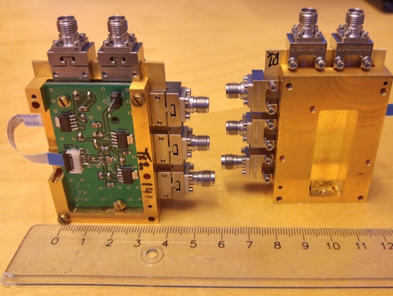 |
| The module above is installed in a link demonstrator at Ericsson out at Lindholmen in Gothenburg. |
He holds up a small module to show the result – it fits in the palm of his hand and is made from machined aluminium parts. On one of the short sides there is a tiny waveguide opening for 110 GHz to 170 GHz, known as the D-band. Inside there is a world-record circuit surrounded by biasing circuits.
“Together with Ericsson we’ve built a demonstrator – a microwave link located out at Lindholmen and which the company uses to showcase to its customers,” Zirath explains.
The demonstrator currently attains 5 Gbit/s, so clearly less than in the lab. The explanation is that the researchers used almost the entire D-band – 60 GHz – when they smashed the world record. That is not permitted commercially, which meant that the research embarked on a different track with the help of Ericsson.
“Instead we’re looking at smaller bandwidths but at more spectrum-efficient QAM-type modulation formats, with more bits per symbol. Our current research is very much geared to increasing the spectrum efficiency, or the number of bits per hertz.”
As small as a sugar cube
The demonstrator at Lindholmen can achieve a link hop of just over ten metres. The current challenge is to increase the distance to 200 m, and after that a few km.
It is primarily the signal-to-noise ratio which determines the hop length, and in highly simplified terms it is the output power from the transmitter and the noise factor in the receiver that determine the result. The snag is that the higher you ramp up the frequency, the harder it is to generate an output power.
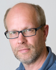
Herbert Zirath |
| Post/title: Professor of High Speed Electronics at Chalmers. Born: 1955. Lives: House in Mölndal. Family: A wife and two daughters, one grandchild. Interests: Plays trumpet in symphonic wind music and big band jazz, downhill skiing, tennis, botany. |
“If you want to improve the spectrum efficiency, it places more demands on the circuit. It’s been a challenge to understand which parameters are most important and what needs to be improved, but we’ve come to the conclusion that the main challenge is to get the noise level down.”
“We’re working hard on this and have started a new activity here to tackle the problems. We’re currently working on the development of the next generation of chips with the aim of increasing the link hop to several kilometres.”
The above-mentioned SSF project includes many parallel activities. Apart from designing a circuit, modem, antennas and encapsulation, it also includes the study of frequencies up to 500 GHz. At the time of writing Teledyne has just delivered the first 500 GHz circuits, which will be tested in the lab.
Another interesting and similar project is M3TERA. It is aimed at creating a more cost-effective and compact means of construction in the THz spectrum, and is part of the EU’s Horizon 2020 framework programme.
Here the indium phosphide chip has had to give way to a silicon germanium (SiGe) circuit manufactured in Infineon’s BiCMOS process B11HFC. The advantage is that more digital functions, as well as processors, can be incorporated into silicon and silicon is also cheaper in higher volumes.
The researchers in this project are working on reducing the size of the module through MEMS technology, in which waveguides, phase shifters and so on are etched in silicon. The MEMS design is a collaboration with KTH Royal Institute of Technology.
“Today we’ve got prototypes on a module the size of a sugar cube, but this isn’t fully functional yet. We’re hoping it will be by some time around the middle of the year. Then we can test it and do a link hop.”
Indium nitride is another material being studied in the MC2 lab. Since indium nitride transports electrons five times faster than silicon, the material is tailor made for circuits in the radar and communications systems of the future.
Kick-off for new competence centre
Researchers working on the five-year “Bridging the THz Gap” project – funded with just over SEK 35 million from the Wallenberg Foundation – are developing an indium nitride material which can in future be used for transistors that will have a large enough output to operate mobile data traffic in the 100 GHz to 1 THz frequency range.
“But growing indium nitride in a controlled manner is a challenge. This is a longer term project which is aimed at developing some sort of material that can be used for transistors.”
The project is a collaboration between Chalmers, Linköping and KTH, and is in its last year. This does not, however, mean that there will be a slowdown in Swedish indium nitride research.
On the contrary, a new competence centre called C3NiT focusing on III-nitrides is about to take shape. It will receive annual funding from Vinnova of up to SEK 7 million over ten years, money which will also be matched by industry.
“The parties signed the consortium agreement late last year so we can now go ahead and get to work,” Zirath says.
C3NiT is to some extent taking over the baton from the Gigahertz Centre, which ran for many years, originally under the name of CHACH – Chalmers Centre for High Speed Technology. Last year the Gigahertz Centre received its final stage of funding from Vinnova of SEK 35 million, which will last until 2021.
A baseplate to stand on
The new competence centre covers a wide spectrum. Materials for both high-frequency and power electronic components based on III-nitrides will be developed here. As an example, in the HF segment Zirath is including future integrated circuits which can replace travelling-wave tube (TWT) amplifiers for space systems.
“TWT amplifiers limit the service life of today’s satellites and they would be best replaced by GaN transistors. RUAG is one of the companies interested in this type of component.”
C3NiT is a collaboration between Chalmers University of Technology and Linköping University. Ericsson, ABB, Saab, ON-semiconductor, UMS, Gotmic, SweGaN, and Epiluvac are the industrial partners.
“It should be seen as a kind of hub around which other projects can be built, such as the Horizon 2020 project and other Swedish projects. It’s important to have a certain baseplate to stand on. The SSF project that I talked about is one such baseplate.”
You can understand that a lot of projects are needed to maintain a research team of around 40 people – half of whom are doctoral students – which Zirath is responsible for keeping employed.
Expertise prized in industry
His tasks also include looking after some 25-30 students who each year choose the Chalmers Master's programme specialising in microwave photonics and space engineering. Zirath states that there is a great demand in the Gothenburg region for engineering graduates who have the expertise he is pioneering.
“Yes, it’s is relatively large job market. We have many large companies such as Saab, Ericsson, Volvo and RUAG, but also a large number of smaller ones with a need for this type of education.”
As examples of smaller scale potential employers he lists Omnisys, which develops spaceborne radiometers, Low Noise Factory which develops indium phosphide HEMTs and delivers extremely low-noise amplifiers that can be used for radioastronomy or quantum computers, as well as Gotmic, Gapwaves and Bluetest.
The last two companies were launched by the late Chalmers professor Per Simon Kildahl. Zirath himself helped to set up Gotmic, while Low Noise Factory is also a Chalmers spin-off from Zirath’s group.
