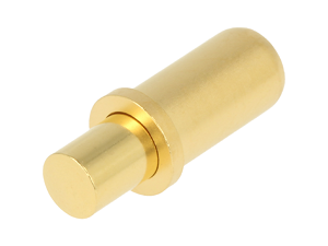
Electronic circuit testers are made of a lot of components – holders, controllers, measuring circuits, sensors. They also contain one essential operating element: test probes.
Production of electronic circuits on a mass scale requires far-reaching automation. This applies to the manufacture of PCBs, the placement of components, as well as their soldering. However, even the most efficient production process can be slowed down at the final quality control stage. That's why advanced ICT (In-Circuit Tests) solutions, which verify a circuit and its parameters through an automated series of measurements, are being used more and more on production lines. Obviously, this type of inspection has been performed for decades – but the increasing miniaturisation of electronics requires ever more precise probing of PCBs and wire harnesses. In the era of communication circuits operating at enormous frequencies, the measurements themselves must also be more accurate, while the general use of digital circuits has irreversibly changed ICT methodologies. Today we often encounter the abbreviation FCT (functional testing), which refers to the detailed verification of a circuit's operation already in the final production stage, by powering it up and simulating its operation in the finished device.
Electronic circuit testers are made of a lot of components – holders, controllers, measuring circuits, sensors. They are programmable and configurable devices. They also contain one essential operating element: test probes. These are precision, spring-loaded probes designed to make good, but short-lived, contact with circuit elements – primarily the leads of passive components and ICs and areas on a PCB. Besides making measurements and checking the continuity of paths, they are also used for other purposes. They can penetrate connectors and allow contact connection testing without exploiting the socket or plug housing. They are also used in digital electronics, where they are applied, among other things, to program microcontrollers using the ISP (In-System Programming) technique and to carry out tests by communicating with the systems installed in the circuit (e.g. by means of a serial port or the CAN bus in the automotive sector). Specialised contact probes are used in the manufacture of batteries, or rather cells and packs, which need to be charged to the optimum level for storage and transport before being stored. An important area of application for contact probes is in electronic services, where automated circuit testing can speed up the process of fault detection and rectification.
Contact probes – the basic parameters
The first difference between the contact probes can be seen at a first glance. This is the shape of the tip (head). We will discuss the purpose of individual heads later in this text. We will first focus on the electrical and mechanical parameters, which should be taken into account in the context of the type of test performed.
As probes are subject to constant use and pressed against PCB components over and over again, they are subject to wear and contamination. Nowadays, with the electronics industry commonly turning to lead-free binders (harder and requiring more chemically aggressive fluxes), the hardness and coating of the contact probes plays a particularly important role. Therefore, we often encounter steel probes and probes made of beryllium copper (CuBe), an alloy characterised by high durability and electrical conductivity comparable to pure copper. To protect the tips from corrosive influences, the probes are usually coated with gold or nickel – in this way they retain their durability even in frequent contact with fluxes and their solvents.
It is important to pay attention to the fact that a simple zero-one continuity test can be performed with probes of relatively high resistance. However, a detailed circuit inspection (or calibration) will rely on a precise measurement whichrequires connections with the lowest possible resistance. Therefore, the nominal resistance will be found in the characteristics of all contact probes. Here, a related factor is the lateral spring deflection – as only the pressure according to the manufacturer's recommendations guarantees obtaining a connection with the specified resistance (working deflection will occur after applying a power determined by a separate parameter). Please beware: (1) the spring compression should not exceed the maximum stroke (in such a situation the probe will not be cushioned); (2) the pressure force is transferred to the components of the tested circuit – an incorrectly selected probe may damage components, paths, etc.
The last important parameter isacceptable working temperature – because automated tests are sometimes carried out between circuit production steps or shortly after the reflow soldering process. In other words, there are situations where the probe is in contact with high temperature components. This also applies to the conditions of so-called stress tests and environmental tests, when the behaviour of a circuit subjected to maximum loads or under extreme thermal conditions is examined.
When selecting probes for testing circuits with a high density of components, another parameter will be important – the minimum pitch in which a given probe can operate.
Application and types of test probes
Electronic circuits are most often probed:
- in specially designated areas (test pads), which in precision electronics are often covered with gold plating (Fig. 1b, 1c, 1d);
- on connections between PCB and leads of components (Fig. 1e);
- VIA points (Fig. 1a), i.e. sleeves connecting PCB layers (most often we are dealing with double-sided boards, but in case of computer or mobile phone motherboards, for example, circuits consist of more layers);
- on contacts of pin connectors and similar connectors (Fig. 1f).
Depending on the point to be tested, as well as the need (or lack thereof) to penetrate deposit, oxidised solder or flux residues, a probe with the proper head shape should be selected to perform the test. So let's take a look at what functions are provided for each solution.

Fig. 1. Test pads of electronic circuits.
Cylindrical or hemispherical probes
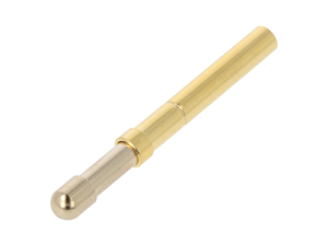
Probes equipped with cylindrical, flat (Figs. 2, 3) or hemispherical (Figs. 4, 5) tips are a safe tool for probing test pads** (especially those gold-plated and cleaned). Hemispherical tips can also be successfully used for measurements made on solder leads or the leads themselves. The overriding feature of such tips is non-invasiveness.
Rounded tip prevents scratching the tested components.
TME also offersprobes with a cylindrical tip with a tapered flute (Fig. 6, 7). This shape facilitates tests carried out on male pin connectors or in place of assembly of THT elements. The wide opening allows to "grab" leads even if they are bent or placed imprecisely. Specialists point out that the tapered flute can quickly become contaminated – if the probe is operated in sub-optimal conditions or in testing services for used and dirty equipment. Nonetheless, it is one of the most popular solutions for the verification of through-hole circuits. Similar properties are found in radial milled heads (Fig. 8) – while also being compatible with flat and convex test points.
Fig. 2
Fig. 3
Fig. 4
Fig. 5
Fig. 6
Fig. 7
Fig. 8
Multi-purpose probes
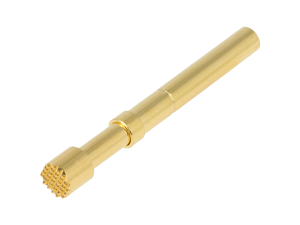
The tips described above have one flaw that can prove critical in manufacturing processes using lead-free solder. Their design makes it difficult for deposit and flux residues to penetrate. As an alternative, cylindrical probes, the top of which has been milled to produce a matrix of pyramids, are available. Not only can such probes be used to connect to most test points (test pads, THT leads, etc.), they also penetrate the top layer of binder (e.g. oxidised), which reduces the risk of test result falsification.
Numerous vertices facilitate contact with both flat and vertical elements.
Fig. 9
Fig. 10
Fig. 11
Conical tips
Conical tips are the oldest and still the most widely used solution. It is important to bear in mind that they have their limitations and are a diverse product group.
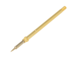
The cone-shaped tips (Fig. 12, 13, 14) can be used for almost all types of tests, although they require precise positioning. Even small variations in PCB size will quickly lead to a series of incorrect measurements. The 60° and 90° bevelled ends are mainly used for testing VIA points and female connectors. Before application soldermasks can also be used to create temporary connections to a single circuit path. Again it should be noted that for bushings and connectors where the surface may be contaminated in some way the milled/fluted types (Fig. 15, 16, 17) are the best option as their edges facilitate penetration.
Precise cone, i.e. for testing of hollowed components.
The best deposit penetration in this product group is ensured by bevelled probes with an angle of 30° or even 15°. These include TEKON probes with heads 13 and 14 as well as the sharp probe 44.118.10.15 from FIXTEST (Fig. 18). These kind of probes are not recommended for testing VIA points filled with solder, because they can damage the connection between PCB layers.
A special case of contact probes with a conical tip are those with a bevelled tip (Fig. 19). Their shape allows connections to be made to many types of test points, they are the most reliable method for testing sockets, and they offer a relatively large contact area and therefore: low resistance and higher current capability.
Fig. 12
Fig. 13
Fig. 14
Fig. 15
Fig. 16
Fig. 17
Fig. 18
Fig. 19
Crown-milled probes
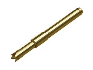
It can be said thatcrown-milled probes (usually with four vertices) combine the benefits of all the solutions presented above. Although not designed for testing VIA points and female connectors, they offer: excellent penetration of coating and deposits; their numerous sharp edges make it difficult for contaminants to adhere (self-cleaning effect); surrounding the central point of the head with vertices makes it easier for the probe to contact the leads of THT components even in the case of minor assembly imperfections (bending, displacement), and focuses the probe on convex test pads.
TME offers probes with a soft (shallow, Fig. 20, 21) and sharp (Fig. 22, 23) crown tip, as well as a three-point variant (Fig. 24).
Fig. 20
Fig. 21
Fig. 22
Fig. 23
Fig. 24
Special purpose probes
In addition to probes for basic electrical testing, TME's range also includes specialised probes for precision measurement, LED testing and (rechargeable) battery handling.
Automated four-wire sensing
Four point/four-wire sensing involves applying four probes to a section of a circuit. The outer pair allows current to flow through the component under test, while the inner pair is used to measure the potential difference at the input and output of the component. With the current and voltage drop data, the meter determines the resistance of the probed object with high precision. Unlike a two-point sensing, the result will not be biased by the resistance of the probing leads – which is why this technique is most commonly used to test low resistances as part of testing and calibration of precision electronics (e.g. measuring devices). This method is often called Kelvin (or Kelvin) sensing/system.
To carry out four-wire sensing, a special type of contact probes is needed, each of which is equipped with two independent contacts. The elements are adapted to perform measurements on connectors and test points especially designed for this purpose. The gold plating and the material ensure repeatability and low connection resistance – even with a large number and high frequency of connection and disconnection cycles.
LED testing
LED testing under mass production conditions is based on (1) electrical measurements and (2) applying power and verifying that the light emitted by the LED has the correct brightness and colour. Functionality testing also verifies that the indicators are properly communicating the status of the device. To verify the operation of the diode, special contact probes are applied to the LED and the emitted light is transmitted through an optical fibre. Further measurements are taken by a sensor placed at the other end of the optical fibre (usually measuring both the intensity and wavelength of radiation). The fibre-optic tip attached to the probe is usually located in a groove that restricts the inflow of external light, so that the test does not need to be carried out in darkness.
At TME we offer a selection of TEKON brand LED contact probes with diameters from 1.1mm to 5mm. This range coincides with the most popular sizes of light emitting diodes – from SMD components to standard THT controls.
Battery probes
Another specific type of contact probes are items designed to create temporary connections to power source terminals. These types of probes are used when testing common consumer batteries (AA, AAA, etc.) as well as rechargeable batteries. Since all cells have an optimum degree of charge in which they should be stored, probes adapted to battery terminals are also used in the process of pre-charging batteries (in the last stage of production), which allows their safe storage and transport.
The large surface area and spring compression force guarantee a good attachment to the terminal.
Battery probe tips are usually cylindrical or hemispherical in shape. Since the size of power sources is strictly defined by international standards, battery probes are characterised by a low spring compression.
Text prepared by Transfer Multisort Elektronik Sp. z o.o. The original source of text: https://www.tme.eu/en/news/library-articles/page/43763/test-probes-types-and-application/
